發布日期:2021-01-22 瀏覽量:3389

關于英諾賽科
關于ASML
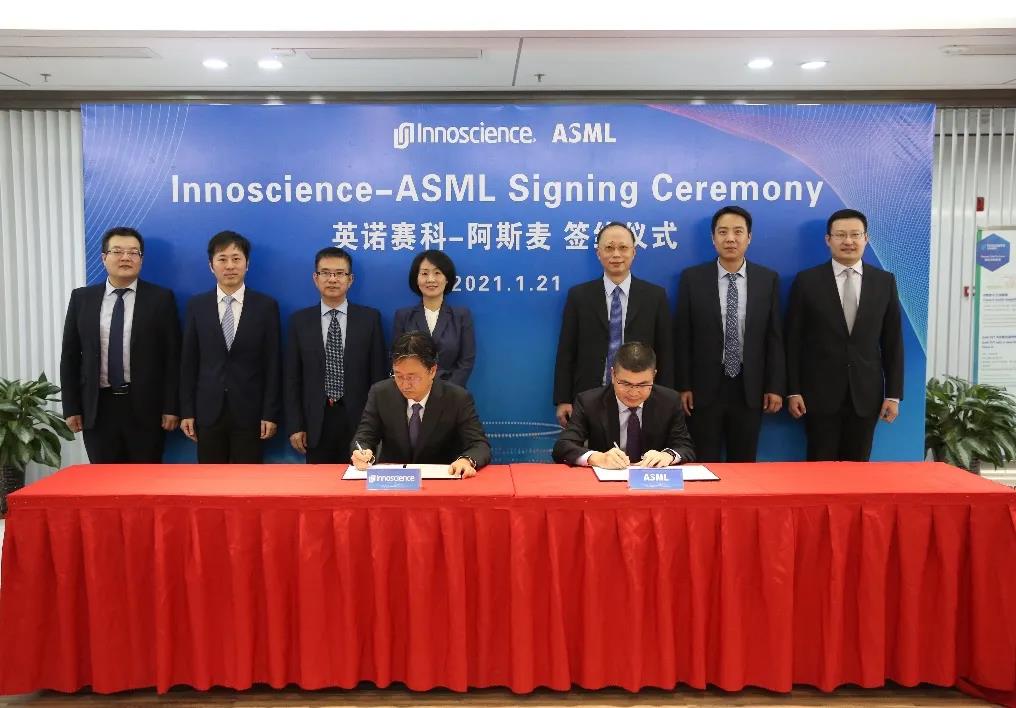
January 21, 2021 – InnoScience and ASML reached a volume purchase agreement for upgraded versions of high throughput i-line and KrF TWINSCAN scanners for advanced GaN on Silicon power semiconductors
Leading GaN-on-Silicon Integrated Device Manufacturer Innoscience Technology Co., Ltd. (“Innoscience”) has recently purchased several TWINSCAN scanners from ASML Holding N.V. (“ASML”), the world’s leading provider of lithography systems to the semiconductor industry. ASML’s XT: 400 and XT: 860 200 mm i-line and KrF scanners, respectively, will be adapted to manufacture GaN-on-Si Power Devices. These tools will not only offer the best performance, but also the highest productivity and lowest cost of ownership available in the market place. ASML’s dual stage TWINSCAN architecture, currently represents the lithography backbone at most of the 200mm and 300 mm high volume manufacturing sites worldwide. Innoscience will receive the first systems in the second quarter of this year. Innoscience is the world first company in the wide band-gap semiconductor field to apply ASML’s advanced TWINSCAN lithography tool in mass production, this effort will bring the fast growing industry to a new era.
Lithography equipment for growing megatrends
Innoscience, which was founded in December 2015, is a company dedicated to developing GaN on Si power solutions. Innoscience successfully established the world first 200mm GaN-on-Si Power Device mass production line, to provide a wide range of product including 30V-650V GaN-on-Si power devices. Innoscience product design and performance have reached international advanced level and are currently widely available in Power Delivery charger, 3D camera, portable device including smart phone, laptop, tablet, etc. Innoscience is committed to build a world-class brand and contribute to the wide band-gap semiconductor industry and its eco-system.
GaN-based power devices and circuits enable high switching frequencies and efficient energy management with high power densities. These features are required for rapidly growing applications such as data centers, renewable energy and the next generation of wireless networks. Alongside the much smaller size factor, GaN-on-Si is an ideal candidate for rapid charging and car electrification. Gallium nitride (GaN) is also called “third generation semiconductor”, together with other materials like e.g. silicon carbide (SiC), aluminum nitride (AlN), diamond, and zinc oxide (ZnO).
Chosen by the best in the industry
Jay Son, CEO of InnoScience, said: “I’m honored to announce Innoscience and ASML have entered into a partnership aimed at changing the future with GaN technology. As an innovation leader in the third generation semiconductors, Innoscience needs strong partnerships to fast advance its technology. By creating a cutting-edge solution together with ASML, we will offer added value to our customers, partners, and consumers in fast growing applications such as quick chargers, time-of-flight (ToF) camera, smart phones, electric vehicle, data center, etc. Together, Innoscience and ASML will develop the next-generation of GaN devices, to provide advance solutions to future power world.
Bo Shen, ASML VP and Country Manager of China said, "We are very happy to be a partner of InnoScience. The third generation of semiconductor materials has broad application prospects in the global market. ASML is committed to support customers in this field, with our broad suite of holistic lithography systems and services."
“Our TWINSCAN 200 mm XT scanner platform, including i-line, KrF and dry ArF product lines, is the ideal long-term solution for the rapidly growing GaN-on-Silicon market, not only in terms of productivity and cost of ownership, but also in terms of overlay and imaging requirements, which will evolve over time, as GaN technology is adopted across new applications” said Toni Mesquida Kuesters, Senior Director of Product Marketing & Business Development for DUV Business Line at ASML. “We are committed to help InnoScience achieve their envisaged goals and, and look forward to a fruitful cooperation.”
About Innoscience
Innoscience is an Integrated Device Manufacturer (IDM) company founded in December 2015. With the development of new technologies, the electric power grid across the world is undergoing a massive transformation. Our vision is to create an energy ecosystem with most effective and low-cost Gallium Nitride on Silicon (GaN-on-Si) power solutions. Innoscience first established a mass production line of GaN-on-Si devices in Zhuhai. In order to fulfill the rapidly growing power demands, Innoscience has inaugurated a new facility in the Suzhou in 2020. As a cutting-edge GaN technology provider, Innoscience’s IDM model guarantees high performance and reliability GaN power devices that can be used in various technical fields as cloud computing, vehicle, portable device, etc. For more information, please visit http://www.innoscience.com.cn/.
About ASML
ASML is one of the world’s leading manufacturers of chip-making equipment. Our vision is a world in which semiconductor technology is everywhere and helps to tackle society’s toughest challenges. We contribute to this goal by creating products and services that let chipmakers define the patterns that integrated circuits are made of. We continuously raise the capabilities of our products, enabling our customers to increase the value and reduce the cost of chips. By helping to make chips cheaper and more powerful, we help to make semiconductor technology more attractive for a larger range of products and services, which in turn enables progress in fields such as healthcare, energy, mobility and entertainment. ASML is a multinational company with offices in more than 60 cities in 16 countries, headquartered in Veldhoven, the Netherlands. We employ more than 28,000 people on payroll and flexible contracts (expressed in full time equivalents). ASML is traded on Euronext Amsterdam and NASDAQ under the symbol ASML. More information about ASML, our products and technology, and career opportunities is available on www.asml.com.
上一篇:氮化鎵下一個風口:PC電源!